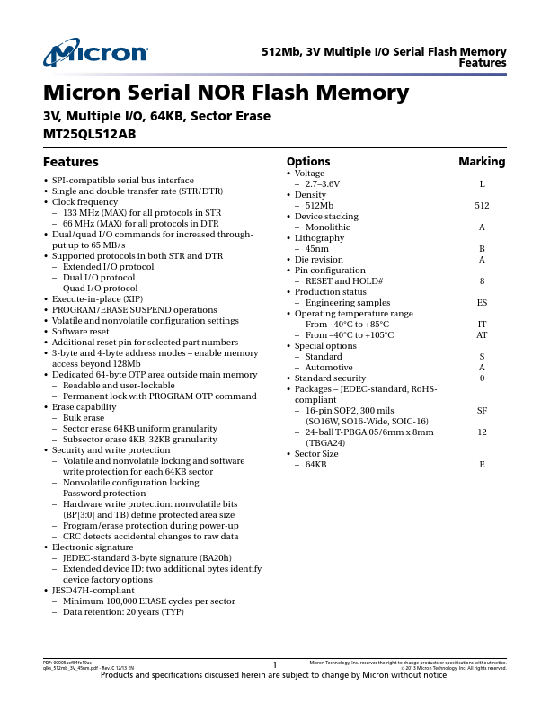
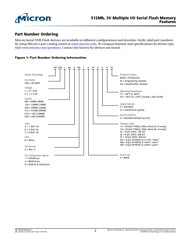
512Mb, 3V Multiple I/O Serial Flash Memory
Features
Contents
Device Description ........................................................................................................................................... 8
Device Diagram ............................................................................................................................................ 8
Advanced Security Protection ....................................................................................................................... 8
Signal Assignments ........................................................................................................................................... 9
Signal Descriptions ......................................................................................................................................... 10
Package Dimensions – 16-Pin SOP2 ................................................................................................................. 11
Package Dimensions – 24-Ball T-PBGA ............................................................................................................ 12
Memory Organization .................................................................................................................................... 13
Memory Map – 512Mb Density ....................................................................................................................... 14
Status Register ................................................................................................................................................ 15
Block Protection Settings ............................................................................................................................ 16
Flag Status Register ......................................................................................................................................... 17
Extended Address Register .............................................................................................................................. 18
Internal Configuration Register ....................................................................................................................... 19
Nonvolatile Configuration Register .................................................................................................................. 20
Volatile Configuration Register ........................................................................................................................ 22
Supported Clock Frequencies ..................................................................................................................... 23
Enhanced Volatile Configuration Register ........................................................................................................ 24
Security Registers ........................................................................................................................................... 25
Sector Protection Security Register .................................................................................................................. 26
Nonvolatile and Volatile Sector Lock Bits Security ............................................................................................ 27
Volatile Lock Bit Security Register .................................................................................................................... 27
Device ID Data ............................................................................................................................................... 28
Serial Flash Discovery Parameter Data ............................................................................................................. 29
Command Definitions .................................................................................................................................... 33
Software RESET Operations ............................................................................................................................ 39
RESET ENABLE and RESET MEMORY Commands ....................................................................................... 39
READ ID Operations ....................................................................................................................................... 40
READ ID and MULTIPLE I/O READ ID Commands ...................................................................................... 40
READ SERIAL FLASH DISCOVERY PARAMETER Operation .............................................................................. 41
READ SERIAL FLASH DISCOVERY PARAMETER Command ......................................................................... 41
READ MEMORY Operations ............................................................................................................................ 42
4-BYTE READ MEMORY Operations ................................................................................................................ 42
READ MEMORY Operations Timings ............................................................................................................... 43
WRITE ENABLE/DISABLE Operations ............................................................................................................. 52
READ REGISTER Operations ........................................................................................................................... 54
WRITE REGISTER Operations ......................................................................................................................... 55
CLEAR FLAG STATUS REGISTER Operation ..................................................................................................... 57
PROGRAM Operations .................................................................................................................................... 58
4-BYTE PROGRAM Operations ........................................................................................................................ 59
PROGRAM Operations Timings ....................................................................................................................... 60
ERASE Operations .......................................................................................................................................... 64
SUSPEND/RESUME Operations ..................................................................................................................... 66
PROGRAM/ERASE SUSPEND Operations .................................................................................................... 66
PROGRAM/ERASE RESUME Operations ...................................................................................................... 66
ONE-TIME PROGRAMMABLE Operations ....................................................................................................... 68
READ OTP ARRAY Command ...................................................................................................................... 68
PROGRAM OTP ARRAY Command .............................................................................................................. 68
ADDRESS MODE Operations .......................................................................................................................... 70
ENTER QUAD and RESET QUAD Operations ................................................................................................... 70
PDF: 09005aef84fe19ac
qlks_512mb_3V_45nm.pdf - Rev. C 12/13 EN
3 Micron Technology, Inc. reserves the right to change products or specifications without notice.
© 2013 Micron Technology, Inc. All rights reserved.